Sign In
Or
Sign Up
Home
Solution
Solution
Layout and process design
Project collaboration and processing
Analysis and testing
Products
About Us
Contact Us
Language
Get a Quote
Language
English
简体中文
Back
Home
Solution
Products
About Us
Contact Us
English
简体中文
Get a Quote
Login
Back
Layout and process design
Project collaboration and processing
Analysis and testing
English
简体中文
Get a Quote
Login
Home
Solution
Layout and process design
Project collaboration and processing
Analysis and testing
Products
About Us
Contact Us
English
简体中文
Language
English
简体中文
Get a Quote
Home
>
Products
>
Testing products
>
KG-12” 3D Tin ball sheet Wafer
KG-12” 3D Tin ball sheet Wafer
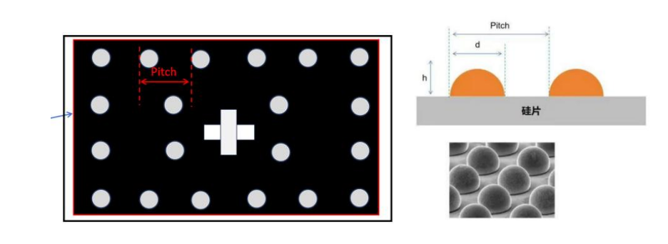
Purpose: The purpose of this document is to generally describe the wafer design and function.
GET A QUOTE
Download
View all downloads
Share
facebook
line
twitter
whatsapp
pinterest
tumblr
linkedin
Description
1.Wafer Introduction
Wafer Size: 12”
Substrate Thickness: 775µm
Substrate Type: P-type lightly doped
Packaging: Single wafer box vacuum sealed packaging
2. Territory
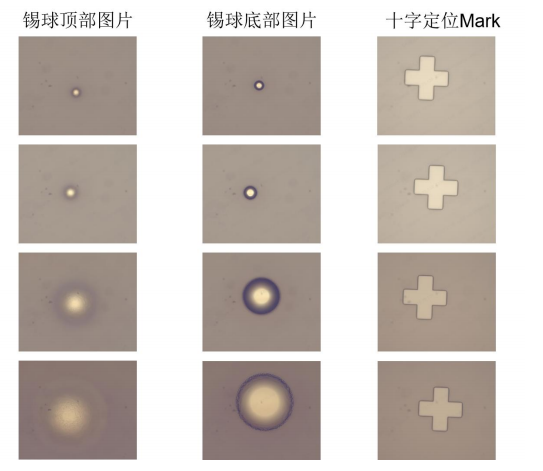
3. Actual measurement images
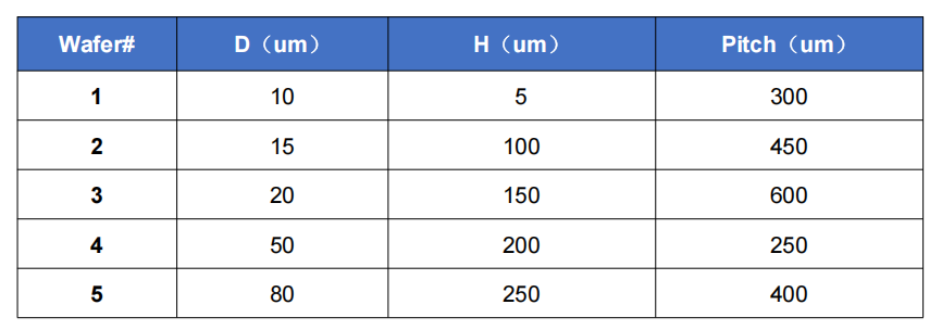
4. Specifications
Feature Products
Visual Check: Cross-section
Visual Check: De-capsulation
Visual Check: AOI
Equipment Name :SAT (Scanning Acoustic Microscope)
Recently Viewed
KG-12” 3D Tin ball sheet Wafer
客户工程师