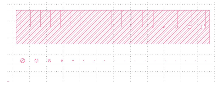
1.Layout: Each shot consists of 4*1 dies, with the defect implanted in the second die. This is used for the Die-2-Die algorithm or the 3-in - 3-out algorithm for defect detection.
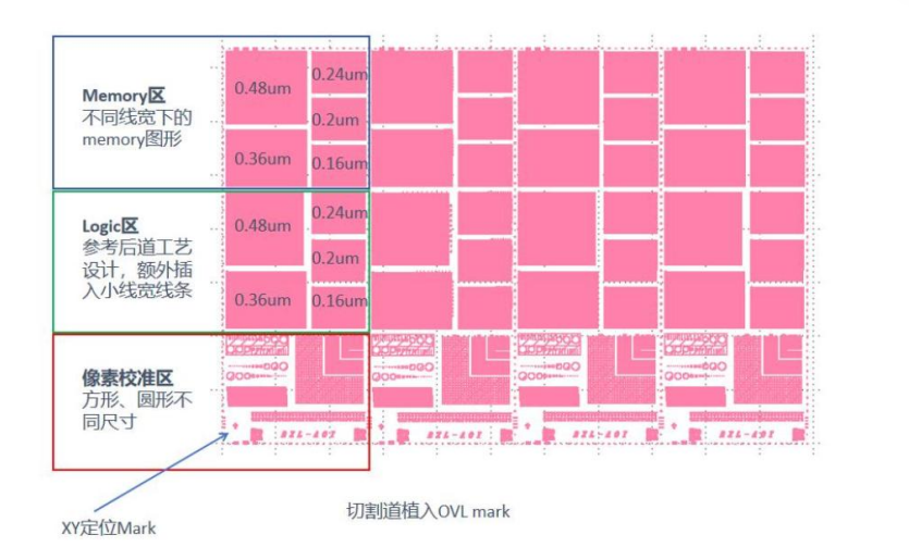
2.The wafer consists of three main regions: the Memory region, the Logic region, and the pixel calibration region.
2.1Memory Region: Used to simulate different standard defects in the memory region during actual production. To simulate defect signals at different production nodes, five linewidths (0.48/0.36/0.24/0.2/0.16µm) were designed. Defects were implanted at each of these linewidths. The line shape in this region is as follows:
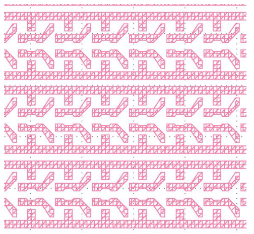
2.2 Logic Region: Used to simulate different standard defects in the logic region during actual production. To simulate defect signals at different production nodes, five line widths (0.48/0.36/0.24/0.2/0.16um) were designed (using the narrowest line width in this region as the benchmark). Defects were implanted at each of the different line widths. The line shapes in this region are as follows:

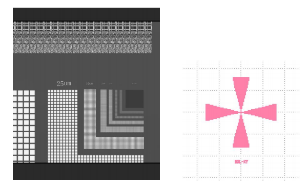
2.3 Calibration Area: This area is designed for camera calibration and includes standard squares, dots, and other elements. Additionally, an XY crosshair positioning mark is embedded for stage positioning evaluation of the equipment.